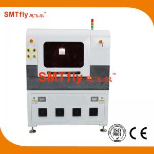
High Precision Pcb Depaneling Equipment All Solid State UVLaser 355nm
Industrial PCB Laser Depaneling
PCB depaneling (singulation) laser machines and systems have been gaining popularity over recent years. Mechanical depanaling/singulation is done with routing, die cutting, and dicing saw methods. However, as the boards get smaller, thinner, flexible, and more sophisticated, those methods produce even more exaggerated mechanical stress to the parts. Large boards with heavy substrates absorb these stresses better, while these methods used on ever-shrinking and complex boards can result in breakage. This brings lower throughput, along with the added costs of tooling and waste removal associated with mechanical methods.
Increasingly, flexible circuits are found in the PCB industry, and they also present challenges to the old methods. Delicate systems reside on these boards and non-laser methods struggle to cut them without damaging the sensitive circuitry. A non-contact depaneling method is required and lasers provide a highly precise way of singulation without any risk of harming them, regardless of substrate.
Challenges of Depaneling Routing
- Damages and fractures to substrates and circuits due to mechanical stress
- Damages to PCB due to accumulated debris
- Constant need for new bits, custom dies, and blades
- Lack of versatility – each new application requires ordering of custom tools, blades, and dies
- Not good for high precision, multi-dimensional or complicated cuts
- Not useful PCB depaneling/singulation smaller boards
-
- Lasers, on the other hand, are gaining control of the PCB depaneling/singulation market due to higher precision, lower stress on the parts, and higher throughput. Laser depaneling can be applied to a variety of applications with a simple change in settings. There is no bit or blade sharpening, lead time reordering dies and parts, or cracked/broken edges due to torque on the substrate. Application of lasers in PCB depaneling is dynamic and a non-contact process.
Specification
| Laser |
Q-Switched diode-pumped all solid-state UV laser |
| Laser Wavelength |
355nm |
| Laser Power |
10W/12W/15W/17W@30KHz |
| Positioning Precision of Worktable of Linear Motor |
±2μm |
| Repetition Precision of Worktable of Linear Motor |
±1μm |
| Effective Working Field |
300mmX300mm(Customizable) |
| Laser Scanning Speed |
2500mm/s (max) |
| Galvanometer Working Field Per One Process |
40mmх40mm |
If you're interested in it,welcome to contact and visit us:
WhatsApp/Wechat(Bunny): +86 136 8490 4990
www.pcb-soldering.com
Email:s5@smtfly.com
www.pcb-depanelizer.com